(1)Unit KMonth
image text translation
(2)Line 1617
(3)20 early-10 late-10 nm level
(4)late 10 nm level
(5)the total of three companies
(6)Global DRAM CAPA
(1)Unit KMonth
image text translation
(2)96th floor, 144th floor.
(3)Micron Singapore
(4)the total of three companies
(5)Global NAND Capa
Approximately 10,000 pyeong of FAB clean room area per 80,000 sheets of DRAM NAND wafer production is required.
From that point of view, Samjeon Xian NAND FAB X1 X2 produces 260,000 wafers per month, so if converted, the area of the clean room is more than 30,000 pyeong.
But Pyeongtaek has 550,000 pyeong of clean room per FAB from P3.
Bigger than P5P6

image text translation
(1)Samsung Electronics Pyeongtaek Campus
image text translation
(2)Two clean rooms on the first floor.
(3)Plant 4 ■■ Plant 6 ■
(4)12 clean rooms
(5)Unregulations to Increase Semiconductor Production
(1)Samsung Electronics Pyeongtaek Campus
image text translation
(2)Two clean rooms on the first floor.
(3)Plant 4 ■ Plant 6 ■
(4)18 clean rooms
(5)Unregulations to Increase Semiconductor Production
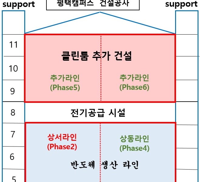
(1)Construction of Pyeongtaek Campus
image text translation
(2)Additional Cleanroom Construction
(3)an electricity supply facility
(4)a semiconductor production line